- PRODUCTS
- RECORDERS
- SUPPORT
| Home > Tutorials > PCI Express: Switched Serial Fabric for the PCI Bus |

Introduced by Intel in 2004, PCI Express is a bidirectional serial link capable of highbandwidth data transfers. Designed to replace the more limited PCI expansion bus, PCI Express supports enhanced features such as power management, hot-swappable devices, and has the ability to handle both host-directed and peer-topeer data transfers. PCI Express can also emulate network environments by sending data between two points without routing it back and forth through the host chip.
Enabling greater bandwidth and performance, PCI Express helps simplify board design and is scalable for future increases in processor speeds and advances in high-performance computing and embedded systems.
Upgraded in 2007, PCI Express 2.0 doubled the data transfer rate over its predecessor for a transfer rate of up to 16 gigabytes per second for a 32X PCIe channel. Providing backwards compatibility with version 1.0, PCI Express 2.0 provides scalable performance, higher bandwidth, lower overhead and lower latency data transfers.
A switched serial fabric system connects devices together to support multiple simultaneous data transfers, usually implemented with a crossbar switch. Using differential signaling, data is sent over a pair of wires at a fixed bit rate such as 1.0 GHz, 2.5 GHz, 3.125 GHz, 5.0 GHz, etc.
The clock, data, and data word framing are encoded into the serial stream, usually with 8B10B coding. Ten bits of serial transmission deliver eight bits of data. The extra two bits maintain synchronization, framing, and DC line balance.

The Serializer shown in Figure 1 encodes clock, frame, and eight bits of data into a 10-bit stream. The Deserializer decodes the 10-bit stream into clock, frame, and eight bits of data. These two functions are usually combined into one device for full duplex operation, known as the SERDES (SERializer/DESerializer).
The raw speed of serial fabrics is governed by three factors:
Peak Rate (MB/sec)=(Serial Rate*Lanes)÷10

Table 1 shows the transfer rates for each link for 1.0, 2.5, 3.125 and 5.0 GHz clocks. The defined clock rates for PCIe 2.0 are 2.5 GHz and 5.0 GHz. With four bit lanes or 4X, the peak transfer rate in each direction with a 2.5 GHz clock is 1.0 GB/sec. With 16X and 5.0 GHz clock, the peak transfer rate reaches 8.0 GB/sec.
Conceptually, the PCIe bus can be thought of as a ‘high-speed serial replacement’ of the older parallel PCI/PCI-X bus. At the software level, PCIe preserves compatibility with PCI: a PCIe device can be configured and used in legacy applications and operating systems which have no direct knowledge of PCIe’s newer features. In terms of bus protocol, PCIe communication utilizes point-to-point switched serial links.
If you bought a desktop PC with Windows OS in the last couple of years, it most likely came with a PCIe graphics card.
This development led to the rapid acceptance of PCIe at the consumer level, as the only bus that could accommodate increasingly faster graphics speeds. The high-bandwidth PCIe interface and fast dedicated graphics board memory made the better PC graphics possible.
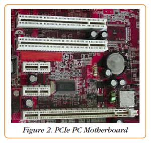
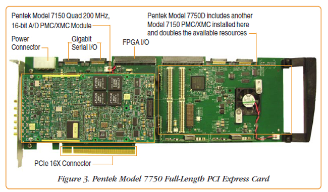
Inside a PCIe PCLooking inside a desktop PCIe PC we see the familiar motherboard, part of which is shown in Figure 2. At the top of the photo, we see the two familiar PCI connectors where you’d find most of the legacy PCI expansion cards, such as sound or 100BaseT Ethernet. Next to these PCI connectors are two small 1X PCIe connectors and at the bottom of the photograph we see a PCIe 16X connector. This is where the video card or the Pentek full-length PCIe board shown in Figure 3 plugs in. A PCIe card will fit into a slot of its physical size or bigger. It will not fit into a smaller PCIe slot. Some slots use open-ended sockets to permit physically longer cards and will negotiate the best available electrical connection. |

|
The number of lanes actually connected to a slot may also be less than the number supported by the physical slot size. An example is an 8X slot that actually only runs at 1X; these slots will allow any 1X, 2X, 4X or 8X card to be used, though only running at the 1X speed. The advantage gained is that a larger range of PCIe cards can still be used without requiring the motherboard hardware to support the full transfer rate, thereby keeping design and implementation costs down.

A PCI to PCIe bridge translates PCIe packets back into regular PCI signals, and allows a legacy PCI device to be plugged into a PCIe system. This bridging can happen anywhere, on the motherboard or on the card itself.
Some companies took this approach with their first-generation PCIe cards. There’s a PCIe-to-PCI bridge embedded on the card, which means that the card itself is still a “PCI” card even though it fits into a PCIe slot. Other companies have cards that support PCIe natively and therefore don’t need the bridge chip.
These bridges do not make any difference as far as PCIe operation is concerned. As a result, they allow the adaptation of legacy cards in PCIe systems at reduced risk and development cost.
Three months ago, Pentek entered the PCI Express market by introducing a family of full-length PCIe boards, each offered in single- and dual-resource versions.
Five products are offered as follows:
The rest of this issue is dedicated to describing in some detail these new additions to the growing Pentek product line.

| CONNECT ON SOCIAL: |
|
|
|
|