| Home > What's New > Models 7750 / 7750D Quad or Octal 200 MHz, 16-bit A/D with Virtex-5 FPGAs |
 | |||
|
Spring 2009 Vol. 18, No. 1 | |||
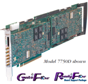
Models 7750 / 7750D Quad or Octal 200 MHz, 16-bit A/D with Virtex-5 FPGAs - PCIe
General InformationModel 7750 is a high-speed data converter suitable for connection as the HF or IF input of a communications system. It features either four 200 MHz, 16-bit A/Ds (Model 7750) or eight A/Ds (Model 7750D). These are supported by an array of data processing and transport resources ideally matched to requirements of high-performance systems. The 7750 attaches to motherboards with full length PCIe (PCI Express) interface slots for installation in various PCs, blade servers and computer systems. A/D Converter StageThe front end accepts four or eight fullscale analog HF or IF inputs on front panel SMC connectors at +8 dBm into 50 ohms with transformer coupling into Texas Instruments ADS5485 200 MHz, 16-bit A/D converters. The digital outputs are delivered into the Virtex-5 FPGA for signal processing or for routing to other module resources. Virtex-5 FPGAsThe Model 7750 architecture includes two (Model 7750) or four (Model 7750D) Virtex-5 FPGAs. All of the board’s data and control paths are accessible by the FPGAs, enabling factory installed functions including data multiplexing, channel selection, data packing, gating, triggering, and SDRAM memory control. GateFlow® FPGA Design Resources facilitate integration of usercreated IP with the factory-shipped functions. There are two FPGA types on the 7750: processing and interface. The processing FPGA serves as a control and status engine with data and programming interfaces to each of the on-board resources including the A/D converters, DDR2 SDRAM memory, interface FPGA, programmable I/O and clock, gate and synchronization circuits. The interface FPGA provides board connections including PCI-X or PCI Express. Implementing the PCI interfaces in this FPGA keeps the processing FPGA resources free for signal processing. The interface FPGA can be configured as an LXT or an SXT family part, providing not only interface functionality, but processing resources up to an additional 640 DSP48E Slices. Memory ResourcesUp to three independent 512 MB banks of DDR2 SDRAM are available to each processing FPGA. Built-in memory functions include an A/D data transient capture mode with preand post-triggering. All memory banks can be easily accessed through the PCI interface using the on-board DMA controllers. PCI Express InterfaceThe 7750 includes a multiple port, 48-lane Gen 2 PCIe switch with integrated SerDes. The switch provides 16X wide connection to the PCIe interface, allowing high-speed data transfers to and from the motherboard. Switch ports each include buffer memory to minimize bottlenecks, with two 4X PCIe connections provided to each FPGA, as well as one 4X connection to each 64-bit PCI-X interface. For more information and price quotation on the Model 7750, click here or on the Model 7750D, click here. 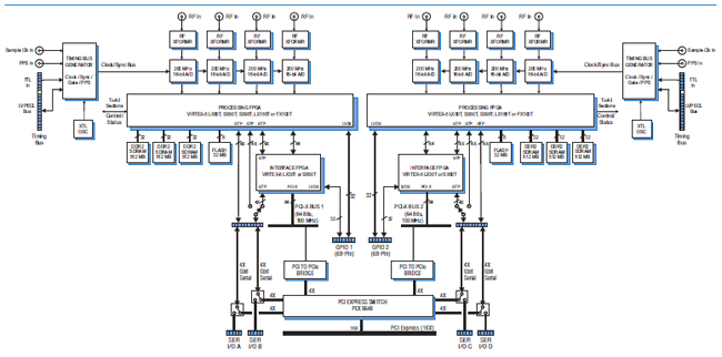 | |||
| CONNECT ON SOCIAL: |
|
|
|
|