New Virtex-7 FPGAs Boost Software Radio Performance
FPGAs have profoundly shaped both the application space and performance levels of software defined radios perhaps more so than any other single technology.
Because today's crowded RF landscape imposes very expensive spectrum allocations for each type of radio, licensed carriers must squeeze as much traffic as possible into their licensed bands. The best solution to this problem is software defined radio systems that utilize digital signal processing techniques to replace traditional analog radio components. They can implement precise, complex modulation schemes to maximize the capacity of a channel while constraining the spectrum to its bandwidth limits.
The latest FPGAs from Xilinx include a host of features specifically targeting the signal processing, control, interface, and data transfer requirements of advanced communications and radar systems. These new features have also dramatically influenced architectures of virtually all new board-level products for real-time embedded systems. This article examines some significant design shifts by system engineers who are now exploiting these new FPGAs to address difficult application challenges.
Virtex-7 FPGAs
The newest generation of FPGAs from Xilinx is the Series 7. It consists of three families each targeting specific price/performance spaces. The Artix-7 family addresses low cost, low power, high volume applications. The Kintex-7 family offers a 2X boost in performance over the Virtex-6 devices. Virtex-7 offers the highest performance of the three families with twice the performance and twice the resources of the Virtex-6.
All Series-7 devices feature low-power 28 nm process technology to implement up to 3.1 Tbits/sec of I/O and over 2 million logic cells. They provide up to 6.7 TMACs of DSP resources, especially important for software radio applications. Because of new process technologies and other power management schemes, they consume half the power of Virtex-6 for a given function.
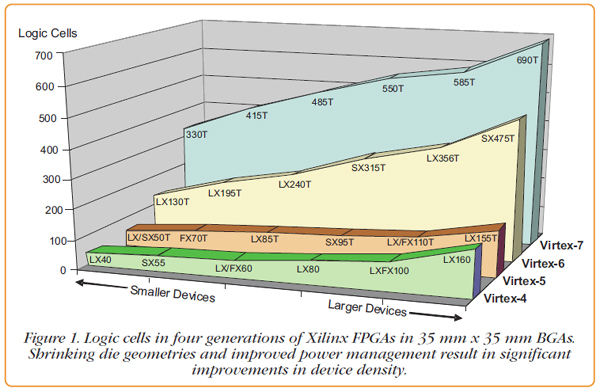
Figure 1 shows the steady improvement in the last four generations of Xilinx FPGAs starting with the Virtex-4 and continuing to the Virtex-7. The graph displays the number of logic cells contained in a range of different density devices offered in a 35 mm x 35 mm BGA package. This clearly shows the dramatic increase in resource density, bounded by the constraints of the size and power dissipation capacity of a given package.
This combination of lower power and higher performance for each of the key resources benefits software radio, opens up new product markets and extends the capabilities of existing applications.
Data Converter Interfaces
To feed the insatiable demand for wireless data service, many newer wideband standards like UMTS and LTE have evolved to deliver data rates up to 1 Gbit/sec. These services require channel bandwidths to 20 MHz and beyond. Other services, such as GSM, operate at more modest channel bandwidths but involve hundreds of channels. For these reasons, one major objective of software radio is to process signals as close to the antenna as possible. This supports flexible software management of the numerous frequency bands; the incorporation of security and encryption schemes; the implementation of various receive and transmit modulation schemes; and beam steering for spatial segregation of radio traffic.
The penalty for putting software radio resources closer to the antenna to handle these wider bandwidths means higher sample rates for the A/D and D/A converters. Early software radio systems operated with modest sample rates of 40 or 65 MHz, but new monolithic data converters are now available with extremely high sample rates.
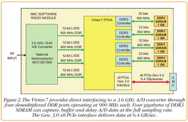
For example, the National Semiconductor ADC12D1800 3.6 GHz 12-bit A/D converter can digitize signal bandwidths of 1.5 GHz. The digital interface splits the data path into four 12-bit demultiplexed outputs, each operating at 900 MHz. Of course, the problem now becomes how to connect these devices to the necessary signal processing elements. At these high-rates, interconnecting traces require controlled impedances, matched lengths, and proper terminations.
Fortunately, the latest Virtex-7 FPGAs provide a direct connection to these types of high-speed peripheral devices with I/O transfer rates reaching 1.866 GHz. To ease the onerous printed circuit board layout constraints, they include per-bit skew adjustments to help align bits in a data word. They also include digitally-controlled termination networks for tuning optimum performance while eliminating the need for external discrete resistors.
Figure 2 shows a Virtex-7 XMC software radio using the 3.6 GHz A/D converter and taking full advantage of the high-speed I/O capabilities of the FPGA.
Memory Interfaces
Synchronous DRAMs offer the densest and most economical solution for large memory arrays. Developed to support highend PC processors, DDR3 SDRAMs deliver extremely fast read/write times to support the high-speed data converters. Data transfers to these devices occur at both edges of the clock, and the latest Virtex-7 devices can support DDR3 devices running bit transfer rates up to 1.866 Gbits/sec. Special FPGA I/O pins allow a direct, glueless connection to these memories.
At these speeds, interface timing for each memory must be carefully tuned for reliable operation. For this reason, DDR3 memory controllers must include high-resolution programmable delay elements and training algorithms, so that optimum timing parameters can be calibrated each time the system is powered up.
Xilinx provides the Memory Interface Generator tool that creates an IP core matching the characteristics of DDR3 devices connected directly to the FPGA. The core includes complete resources for initialization, training and delay leveling for reliable read and write operations. Figure 2 shows direct connections from the FPGA to four 1 GB banks of DDR3 SDRAM capable of capturing, buffering and delaying data samples from the 3.6 GHz A/D in real-time with no data loss.
Data Buffering
Once high-speed peripherals have been successfully interfaced to the FPGA, the designer must deal with managing the staggering flow of data to and from other system resources. While A/D and D/A converters operate at a constant clock rate, networks and system buses transfer data in packets or blocks.
Block RAM resources of FPGAs can be used as FIFOs to provide an elastic-data buffer for some applications. In other cases, a swingingbuffer memory is more appropriate, especially for blockoriented bus interfaces. A swinging buffer, also built from FPGA internal block RAM, allows one memory bank to be filled from one resource, e.g. an A/D converter, while another bank is being emptied by another resource e.g. the PCIe interface. These schemes are extremely effective when the average data rate of a peripheral is less than the average rate of the system interface.
The largest Virtex-7 devices now offer more than 10 MB of internal block RAM, more than twice as much as the previous generation.
However, transient capture applications like radar, require a large amount of data to be captured at a very high rate in real-time during a range gate, even though the duty cycle of the gate is relatively low. In this case, because FPGA block RAM is too small, external memory must be used, and the specialized SDRAM interfaces discussed above come into play. In these applications, duty cycle averaging allows the system interface to operate at a much lower speed with no data loss.
For example, in a radar system, the 3.6 GHz A/D converter XMC module shown in Figure 2 generates sample data at 4.8 GBytes/sec (assuming 1.5 bytes per sample). For a range gate with 100 msec duration, the capture buffer size must be 480 MB, fitting nicely within any of the four 1 GB SDRAMs. If the duty cycle is 10%, data in the buffer must be delivered to the system interface at an average rate of only 480 MB/sec, a reasonable rate for most embedded systems.
Gigabit Serial Links
Traditional parallel buses have become serious bottlenecks because of high-speed peripherals and processors and high-density packaging. Just as desktop PCs have migrated away from PCI and PCI-X towards PCIe (PCI Express), new embedded system architectures abandon parallel backplane buses in favor of switched serial fabrics and gigabit serial links. The two main advantages are higher speed interconnects and multiple simultaneous paths between software radio system boards and components. More than any other device, FPGAs are the enabling technology for this significant transition.
They provide the low-level electrical interface, the SERDES (serializer and de-serializer), and the 8B/10B encoding engine that delivers clock and data over a single differential pair of copper lines. This interface constitutes the underlying physical and transport layers common to most of the popular gigabit serial standards, including Ethernet, Aurora, PCI Express, and Serial RapidIO.
Protocol engines for specific standards can be configured using FPGA logic so that FPGAs can adapt to different protocols as required. They interface to the SERDES and correctly process protocol-specific packets, header information, control functions, error detection and correction, and payload data format. The strategy makes FPGA-based modules truly “fabric agnostic” and allows one hardware design to be deployed in several different fabric environments.
This flexibility in using one hardware product to cover several different protocols encourages board vendors to develop FPGAbased products for the general market. It also affords system integrators the luxury of not having to commit to any particular standard when selecting boards for their systems.
In their latest Virtex-7 devices, Xilinx offers gigabit serial transceivers with four different bit rates: 6.6 GHz (GTP), 12.5 GHz (GTH), 13.1 GHz (GTX) and 28 GHz (GTZ).
PCI Express
Xilinx FPGAs advance gigabit serial technology even further by including integrated PCI interface blocks for PCI Express that incorporate key layers of the PCI Express protocol stack. This saves FPGA resources for other tasks and offers a standardized solution for sending and receiving data using one of the most popular system protocols.
Some Virtex-7 devices now support the PCI Express Base Specification 3.0 with capabilities for both endpoint and root port. Since each generation also accommodates lower generation devices, the Gen. 3 interface which operates at 8 Gbits/sec is backward compatible with Gen. 2 at 5 Gbits/sec and Gen. 1 at 2.5 Gbits/sec.
The integrated PCI interface blocks can be configured for 1, 2, 4 or 8 lanes and advanced buffering schemes raise the size to 1024 bytes for maximum sustained throughput rates.
OpenVPX
OpenVPX is a new embedded system standard well suited for high-density, high-performance applications. Instead of a parallel bus backplane, it uses direct pointto-point gigabit serial links between backplane connectors in a wide range of interconnect topologies. Each link has groups of differential pairs in both directions in 1x, 2x, 4x, 8x, 16x and 32x lane groups, each supporting any gigabit serial protocol.
The VITA 65 OpenVPX specification defines profiles for backplanes, slots, and modules to standardize on the implementation of system components from various vendors to promote interoperability.
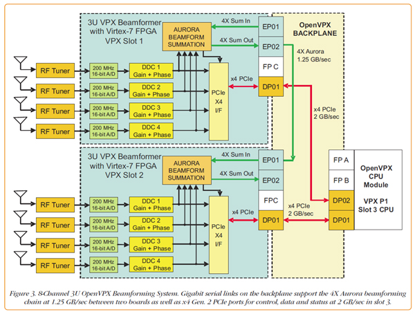
Figure 3 shows a complete 8-channel OpenVPX beamforming system based on two 3U VPX beamformer modules installed in slots 1 and 2 of an OpenVPX backplane, along with a CPU board in slot 3. Eight antenna signals feed RF tuners containing low-noise amplifiers, local oscillators and mixers. The RF tuners translate the antenna frequency signals down to an IF frequency.
The 200 MHz 16-bit A/D converters digitize the IF signals and the DSP48E1 FPGA engines in the FPGA perform further frequency downconversion to baseband. Phase and gain coefficients for each channel are applied to steer the array for directionality. The four weighted baseband signals are summed together. An Aurora engine on each module accepts a sum generated by a previous module and propagates a new sum out to the next module using two 4X gigabit links out to the backplane.
In this system the top left module sends its 4-channel sum to the bottom left module to form the final 8-channel sum. This is delivered to the CPU module in slot 3 over the x4 PCIe interface. In addition, the CPU module uses these PCIe links for initialization, status and control of the two beamformer modules.
Here the Virtex-7 FPGA provides interfaces to the A/D converters; performs the digital downconversion; implements the beamforming phase shift and gain adjustments; sums the channels together; links the summation Aurora chain across the backplane; provides a PCIe interface to the CPU; and implements all control, data flow, synchronization and timing within each module.
Summary
The system example above clearly shows that, except for the A/Ds, every other aspect of the module is implemented with FPGA technology. No other design approach is viable, except for a custom ASIC solution, practical only for high volume production.
When coupled with their impressive DSP capabilities, FPGAs have clearly revolutionized embedded system board-level product design. FPGA vendors continue to compete by offering new features, better performance, higher density, and lower power. To take the best advantage of these powerful components, software radio system designers must constantly keep abreast of frequent announcements.
Pentek Catalogs
All Pentek online catalogs have been recently updated with the latest products:
Product Segment Catalogs
| |
Full Product Catalog
Onyx Virtex-7 and Cobalt Virtex-6 Product Catalog
|
|