|
Spring 2008 Vol. 17, No. 1
Model 7150 Quad 200 MHz, 16-bit A/D PMC/XMC Module with two Virtex-5 FPGAs
General Information
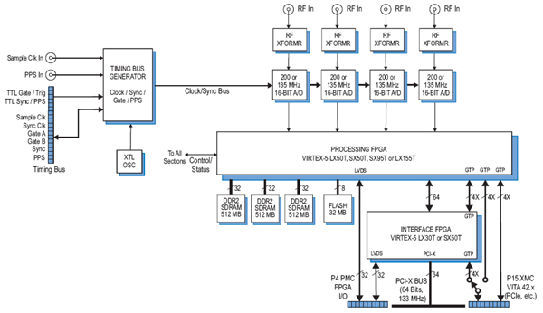
Model 7150 is a quad, high-speed data converter suitable for connection as the HF or IF input of a communications system. It features four 200 MHz, 16-bit A/Ds supported by an array of data processing and transport resources ideally matched to the requirements of high-performance systems.
Model 7150 uses the popular PMC format and supports the emerging VITA 42 XMC standard for switched-fabric interfaces.
A/D Converter Stage
The front end accepts four full scale analog HF or IF inputs on front panel SMC connectors at +10 dBm into 50 ohms with transformer coupling into four 200 MHz, 16-bit A/D converters.
The digital outputs are delivered into the Virtex-5 FPGA for signal processing or for routing to other module resources.
Virtex-5 FPGAs
The Model 7150 architecture includes two Virtex-5 FPGAs. All of the board’s data and control paths are accessible by the FPGAs, enabling factory installed functions including data multiplexing, channel selection, data packing, gating, triggering and SDRAM memory control. In addition to the built-in functions, users can install their own custom IP for data processing. Pentek GateFlow® FPGA Design Resources facilitate integration of user-created IP with the factory- shipped functions.
The processing FPGA serves as a control and status engine with data and programming interfaces to each of the on-board resources including the A/D converters, DDR2 SDRAM memory, interface FPGA, programmable LVDS I/O and clock, gate and synchronization circuits. The processing FPGA can be populated with a variety of different FPGAs to match the specific requirements of the processing task. Supported FPGAs include: Virtex-5 SX50T, SX95T, LX50T and LX110T among others.
The SXT parts feature between 288 and 640 DSP48E Slices and are ideal for demodulation/modulation, decoding/encoding, decryption/encryption, digital delay and channelization of the signals between reception and transmission. For applications requiring more FPGA logic cells, the Model 7150 can be optionally configured with an LX110T in the processing FPGA position for 110,592 logic cells.
A second Virtex-5 FPGA provides board interfaces including PCI-X or PCI Express. Implementing the PCI interfaces in this second FPGA, keeps the processing FPGA resources free for signal processing. The interface FPGA can be configured as a VLXT family or an LXT family part, providing not only interface functionality, but additional processing resources up to an additional 640 DSP48E Slices.
Optionally, the P4 PMC connector may be fitted with 16 pairs of LVDS connections to the processing FPGA and 16 pairs of LVDS connections to the interface FPGA for custom I/O.
Clocking and Synchronization
The architecture includes a flexible timing and synchronization circuit that allows the A/Ds to be clocked by internal or external clock sources and a multiboard timing bus.
|