| Home > Pipeline Vol. 15 No. 1 > Jefferson Lab Advances the State of Science in Nuclear Physics |

| ||||||||||||||||||
|
Spring 2006 Vol. 15 No. 1 | ||||||||||||||||||
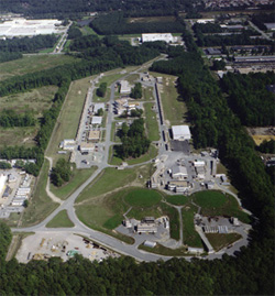
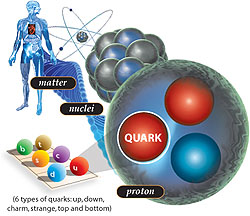
Jefferson Lab Advances the State of Science in Nuclear PhysicsJefferson Lab is a nuclear physics research facility operated for the Office of Science of the US Department of Energy by the Southeastern Universities Research Association (SURA). An international community of about 2,000 scientists conducts research to increase the understanding of the structure of matter and the forces that hold the atom's nucleus together. By smashing electrons into atoms in JLab's Continuous Electron Beam Accelerator Facility (CEBAF) the scientists have already mapped the structure of the proton to an unprecedented level.
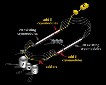
Accelerator PhysicsInside the accelerator, a stream of electrons races around the racetrack. A billion times per second, magnets steer and focus the electrons into a beam the width of a human hair. The accelerator is controlled and monitored by more than one hundred computers. Together, they track, manage and respond to more than 240,000 simultaneous signals and 40,000 hardware control points. Eventually, the electron beam is funneled into three experiment halls where the high-speed particles are slammed into target materials. Scientists from around the world use the electron beam to perform experiments which refine theories about how "quarks", the small particles that combine to form protons and neutrons, behave in the nucleus. By measuring the properties of scattered particles after the electron beam collides with a target nucleus, scientists learn how quarks and the forces that hold them together interact and form the ordinary matter in the universe. Jefferson Lab Upgrade
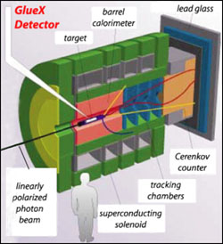
The new experimental hall includes approximately 18,000 Flash* A/D Converter channels (ADC) and 4,300 Time-to-Digital Converter channels (TDC). These ADC and TDC channels are connected to the readout electronic modules that reside in a standard VME card enclosure. The card enclosures are known as "crates" and the new detectors proposed for the experimental hall will need approximately 70 to 80 crates. The crates provide power to the individual modules and establish a high-speed data acquisition path using defined standards for data bus protocol.
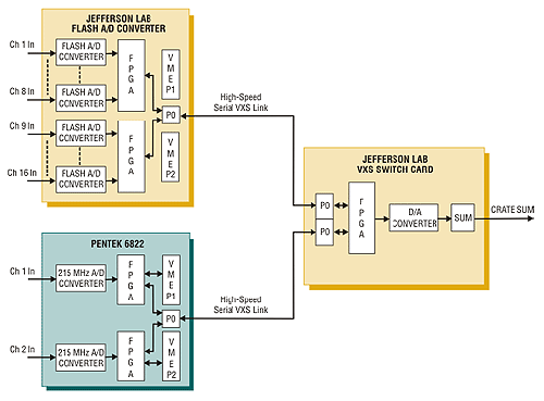
Pipelined Data AcquisitionThe new experimental apparatus, constructed with various particle detectors, requires that the front-end electronic modules support a high trigger rate. Digitization of the input signals for analog pulse information and timing must be buffered for several microseconds, while the overall trigger is formed from all the detector sections. Since multiple signals could not be digitized and stored in the front end modules, the older instrumentation standards did not allow for pipelined data acquisition techniques. The overall data acquisition trigger rate was limited by these non-pipelined modules and remained well below 3 kHz. With pipeline design techniques and improvements in FPGAs, the digitization process can be increased at the front end and the information can be stored until the trigger processing is completed. The design goals for the new experiment are a 200 kHz trigger rate with approximately 5 kbytes of event data. This corresponds to an overall data acquisition rate of 1 Gigabyte per second. Creating the TriggerThe instrumentation modules connected to the detector sections that form the trigger, must transfer information from each module in the crate to a central collection module. Each module produces a digital sum of the signals that are present on each input channel. The sum signal from each module is collected and added to the other modules in the crate. The crate sum is the first level of trigger processing for the overall experiment trigger. All the crates that collect signals from detector sections responsible for the trigger are ultimately summed again to create the "Physics Event" trigger signal. This final trigger signal is distributed to all the front-end instrumentation modules and initiates the readout of stored data in the modules. Designing with VXSThe VITA 41 VXS specification provides the capability for connecting each module in a data acquisition crate with a central collection module. The VXS standard defines high speed, multigigabit serial connections from each VME64x module slots to a central collection module. The Electronics and Data Acquisition groups at Jefferson Lab have embarked on a design that takes advantage of the high speed backplane designs that the VXS standard has created. This standard allows JLab to use legacy VME/VME64x modules in a VXS crate, to develop modules that will be used in the final design of the data acquisition system for the detector systems constructed for the 12 GeV upgrade. Commercial crate and backplane designs to support the VXS specification have been researched at JLab. To support the plans for designing front end electronic modules and testing vendor backplanes, JLab purchased the Pentek Model 6822 Dual Channel 215 MHz, 12-bit ADC VXS board. As shown in Figure 4, it provides the hardware to drive the VITA 41 backplane. The Pentek Model 6822 is unique in that it also allows the user to develop algorithms that can be loaded to the on-board FPGA for signal processing. The preprocessed data is then transferred through the VXS backplane to the central collection module. The 6822 will be used to test data processing routines, and to verify the central collection module development and design effort. CommercializationThrough its technology commercialization programs, SURA is collaborating with other national labs, universities and the private sector to find practical applications for these technologies. Exciting examples include medical imaging for early detection of cancer and security scanning devices. Through the active pursuit of applying research to meet the needs of the commercial marketplace, SURA's technology transfer program seeks to positively impact the economy and improve people's lives in ways that have never been considered before. Also See:
* Flash ADC: Also called the parallel A/D converter, this circuit is the simplest of ADCs. It consists of a series of comparators, each one comparing the input signal to a unique reference voltage. The comparator outputs connect to the inputs of a priority encoder circuit, which then produces a binary output.
| ||||||||||||||||||
 | ||||||||||||||||||
| CONNECT ON SOCIAL: |
|
|
|
|