| Home > Pipeline Vol. 15 No. 4 > Designing a 256-Channel Digital Downconverter |

As Software-Defined Radio technology further penetrates large communication systems for battlefield military radio networks, commercial wireless systems, manned and unmanned aerial vehicles, and monitoring facilities for SIGINT and COMINT, the need to accommodate a large number of agile frequency channels for radio receivers is quite apparent. In each of these applications, the same critical metrics apply: size, weight, power, and cost for each receiver channel.
Traditional Digital Downconverter (DDC) ASIC devices feature only one to four channels per chip, and straightforward implementations of DDCs in FPGAs consume a significant percentage of available resources. A new approach to DDC design takes advantage of the parallelism of FPGAs to create a highly efficient architecture for multichannel receivers.
DDCs, sometimes called digital receivers, perform the two essential software radio functions: frequency translation and channel filtering. In a basic DDC shown in Figure 1, a mixer and local oscillator perform the frequency translation.
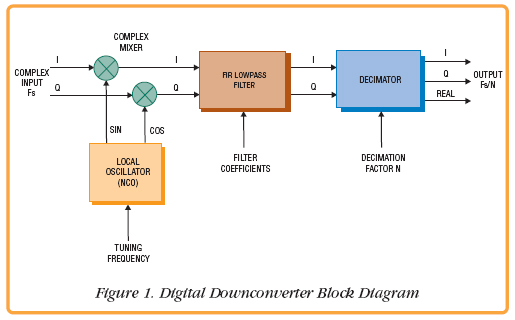
The local oscillator consists of a digital phase accumulator that advances each clock by a programmable increment equal to the tuning frequency. The phase accumulator is a register whose full-scale value represents 360 degrees of a sinusoid. A sine/cosine lookup table converts the phase angle of the accumulator to the digital voltage value of the sinusoid. The higher the increment, the faster the phase accumulator steps through the sine table. It naturally overflows at the top, preserving any residue left in the register as a phase offset for the first sample of the next cycle. As a result, the output sinusoid is directly proportional to the phase increment or frequency setting. This block is a classic Numerically Controlled Oscillator (NCO), also often called a Direct Digital Synthesizer (DDS).
The mixer consists of two digital multipliers that accept complex sine/cosine outputs from the local oscillator and digital samples of the receiver input signal produced by an A/D converter. Multiplication in the time domain produces a sum and difference signal in the frequency domain. If the local oscillator is set to the frequency of the input signal of interest, the difference term will be that input signal translated down to 0 Hz. Since the mixer is complex, the upper and lower sidebands of the input signal will be translated to negative and positive frequencies centered at 0 Hz.
The filter is a complex low-pass digital filter with two parallel I and Q arms whose coefficients are programmed for a passband equal to the channel bandwidth. Because the output of the filter is bandlimited, the output decimation stage can drop the sampling rate accordingly.
DDCs are grouped into two main categories. Wideband DDCs have output channel bandwidths typically above 1 MHz and are appropriate for wideband Code Division Multiple Access (CDMA) and radar applications. Narrowband DDCs with bandwidths below 1 MHz are widely used for Frequency Division Multiplexed (FDM) systems including voice and music channels in telecom and commercial broadcast systems. While the mixer and local oscillator sections are quite similar for all DDCs, the best filter design depends on the filter bandwidth. For wideband channels, a conventional FIR filter, as shown in Figure 1, is best. For narrowband channels, a multistage Cascaded Integrator-Comb (CIC) filter, followed by an FIR filter to correct frequency droop, is more efficient.
For narrowband applications, both ASIC and FPGA Intellectual Property (IP) cores are available using CIC filter designs. Commercial ASICs feature as many as four channels per chip, like the popular Texas Instruments/Graychip GC4016.
IP core DDCs, like the LogiCore DDC from Xilinx for its Virtex-II Pro, can be scaled for various levels of Spurious-Free Dynamic Range (SFDR) performance to use more or less of the available resources. For example, a complex DDC with 84 dB SFDR consumes approximately 1,700 slices. In a mid-sized FPGA device with 24,000 available slices, only about 14 DDC channels can be accommodated. For applications requiring several dozen or even hundreds of channels, this approach can become impractical.
Because of the extremely fine resolution of its NCO tuning frequency, a true DDC can translate any input frequency component down to 0 Hz, often with 32-bit accuracy. This ability makes DDCs ideal for applications that require precise changes in tuning such as in continuous Doppler correction for satellite tracking systems.
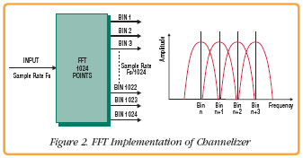
However, in other applications, a channelizer approach may be sufficient. This is a bank of equally spaced, fixed frequency band-pass filters whose outputs are translated to baseband (0 Hz). One crude example of a channelizer familiar to everyone is a simple FFT. It converts a block of N time samples equally spaced in time into block of N frequency samples equally spaced in frequency. For a continuous stream of input time sample blocks, samples at a given point in successive output blocks represent a translated, bandpass frequency signal or bin.
|
By selecting the output of a particular bin, a channelizer can serve as a primitive DDC, but with extremely coarse tuning resolution that is determined by the number of points in the FFT as shown in Figure 2. Another serious limitation of the FFT as a DDC is the frequency response (passband flatness) of the bin, and rejection of energy from adjacent bins (stop-band rejection). |
|
Other channelizer designs use various digital filtering techniques to split the bands with better flatness and adjacent channel rejection, but they usually require significantly more hardware than an FFT for a comparable number of bins. Regardless of its design, the tuning resolution of any channelizer is simply equal to the number of bins or channel filters. As a result, channelizers may be useful for spectrum analyzers, scanners, and energy survey equipment but they are rarely used as substitutes for DDCs in software radio communication systems.
The software radio market generates a growing number of requests for DDC solutions with densities higher than the 16 or 32 channels provided per board using ASICs or standard FPGA designs. Therefore, we embarked on a mission to a new signal processing architecture for a narrowband DDC with 64 channels or more; with full tuning resolution, but with much more efficient use of FPGA resources than deploying a farm of conventional DDC cores.
Each conventional DDC requires its own local oscillator (phase accumulator and sine table), mixer (two multipliers), and FIR filter (multipliers and accumulators). All of this hardware must operate at the full input sample clock rate, and clock rates for A/Ds commonly used in software radios range between 100 and 200 MHz. Since this is the same clock range rating for commercial DDC IP cores, all of the hardware resources used for each channel must be dedicated to that channel.
However, imagine that the input data sample rate is reduced by a factor N. By operating the DDC hardware resources required for one channel at the full clock rate, those same resources can then be multiplexed (time-shared) across N channels. Of course, provisions must be made for buffering the data for all channels while multiplexing. This is usually done in RAM or in delay memory, a common feature of FPGAs.
One way to achieve this input rate reduction is to split the input signal into a bank of N adjacent frequency bands using a channelizer. Then, the output sample rate for each band can be reduced by a factor of N. The output from the band containing the signal of interest can be selected as the input to any given DDC to fine-tune within that band.
The tradeoff question becomes: Are the resources freed up by multiplexing the DDCs more than the resources required for the channelizer? The answer lies in how efficient the channelizer can be.
Figure 3 shows an FPGA-based 256-channel DDC IP core that combines a channelizer stage with a multiplexed DDC stage.
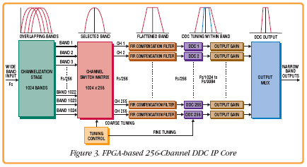
The crucial part of this design is the channelizer stage. It accepts a single wideband input stream and delivers a channel bank of 1,024 output bands equally spaced in frequency, but with significant overlap between adjacent bands.
The output sample rate of each band equals the input sample rate (Fs) divided by 256, rather than 1,024, as would be expected with a simple FFT. In fact, inside the channelizer are four high-speed 1,024-point FFTs running in parallel using a proprietary windowing and overlap processing technique. The outputs of the four separate FFTs deliver samples at a rate of Fs/1024. These outputs are combined to form a single output at a sample rate of Fs/256, which supports the wider bandwidth that will sufficiently overlap adjacent bands.
The next stage is a crossbar switch matrix that accepts 1,024 inputs from the channelizer and delivers 256 outputs, one to each DDC channel. The switch is nonblocking so that any of the 256 outputs can be independently sourced from any of the 1,024 channelizer bands with no restrictions.
Each of the 256 channels is tuned by a separate 32-bit frequency word, with the most significant bits sent to the switch matrix for coarse tuning. This selects the correct channel band for each channel. The least significant bits of the frequency word are used by the DDC stage for fine tuning within the selected band.
Because the channelizer outputs exhibit frequency droop at the band edges, a fixed compensation FIR filter flattens the passband to within 1 dB across a span equal to twice the band-to-band spacing.
A bank of 256 independently tuned DDC sections, each with its own local oscillator, mixer, and FIR filter processes the 256 compensated switch matrix outputs. Because the channelizer has dramatically reduced the input sampling rate to each DDC section by a factor of 256, the DDCs are implemented using highly multiplexed hardware resources and block RAM to preserve the data for each channel. A gain stage, output multiplexer, and data formatter complete the design.
The maximum output bandwidth of this design equals the channelizer band-to-band spacing of Fs/1024. For an input sample rate of 100 MHz, this spacing is about 100 kHz. And because of the broadened response, each channelizer output has a clean passband equal to twice the band spacing, or about 200 MHz.
This allows the DDC to perform fine tuning by sliding its local oscillator frequency ± 100 kHz across the selected 200 kHz channelizer band to precisely center the DDC output. Choosing a wider DDC output bandwidth would restrict the DDC tuning range, since the edge of that wider bandwidth would cross the edge of the flat, spurious-free region of the channelizer output.
Samples of the translated signal from the mixer arrive at the decimating FIR at the channelizer output sample rate of Fs/256. Since the maximum available DDC output bandwidth is Fs/1024, the lowest decimation factor allowed in the FIR is 4.
For narrower output bandwidths, the maximum decimation factor is determined by the complexity (number of taps) of the FIR filter, which must perform at least as well as the channelizer filter in order to maintain the dynamic range of 75 dB.
Choosing a reasonable number of multiplier/accumulator stages, yields an FIR filter suitable for decimation factors from 4 to 39 in steps of 1. The number of filter taps is equal to 26 times the decimation factor of the filter.
|
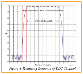
Since the channelizer decimation (256) and FIR filter decimation (4 to 39) multiply, the overall range of decimation range for the entire core is 1,024 to 9,984 in steps of 256. Each of these 36 available decimation factors requires its own set of filter coefficients, which are stored in a table within the FPGA. For an input clock of Fs = 100 MHz, the range of output bandwidths using the default 80 percent filter characteristic is approximately 8 kHz to 80 kHz. For any decimation setting, the overall DDC channel characteristics including the channelizer response, are shown in Figure 4. |
|
Because of the multiplexed DDC hardware, all 256 channels must have the same decimation factor setting. For high-channel count systems, this limitation is usually not an issue since it is quite common for all such channels to have the same bandwidth.
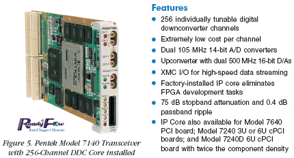
Overall performance of the complete 256-channel FPGA-based DDC IP core includes a spurious-free dynamic range of 75 dB, a passband ripple of 0.4 dB, a passband edge droop of 1.0 dB, and frequency tuning resolution of Fs/232. The maximum clock frequency depends on implementation details, but can be as high as 185 MHz in a Virtex-4 FPGA with speed grade 12.
The core consumes approximately 18,000 logic slices of a Virtex-4 device, compared to 1,700 slices for a single channel DDC Logi-Core reference design. Although there are some limitations in decimation factors and dynamic range, this new core represents an improvement in the channel-per-slice ratio by a factor of more than 20.
This 256-channel DDC core is suitable for use with any Virtex-II, Virtex-II Pro, or Virtex-4 product.
For customers preferring to avoid FPGA development, it can be ordered as a factory installed option to the Pentek Model 7140 Dual Transceiver PMC module, shown in Figure 5, where it occupies approximately 76 percent of the Virtex-II Pro XC2VP50.
In order to keep pace with a steady flow of new FPGA device offerings, designers must continually evaluate, and often reinvent, real-time embedded computing strategies for critical military and commercial applications. Armed with a detailed understanding of new device resources, creative engineers can often approach a tough problem from a radically new angle to gain a major advantage. While many new FPGA design tools offer impressive features and improved efficiencies, these truly significant leaps in FPGA performance usually come from inspiration, not from automation.

| CONNECT ON SOCIAL: |
|
|
|
|