Selecting the Right FPGA for Your Application
Field Programmable Gate Arrays (FPGAs) are a tremendously exciting implementation platform. They are used to replace Application Specific ICs (ASICs), such as digital receivers, and programmable general purpose processors or DSPs.
Even though programmable logic has been around for many years, the latest generation FPGAs are more powerful and are making their way as the right solution for many embedded applications.
Each new generation of FPGA devices delivers faster speeds, improved density, larger memory resources and more flexible interfaces.
Embedded system board vendors face a difficult challenge, since each customer has a different mission unknown to the board designer at the time FPGA component selection is made. Successful new product definition requires an intimate knowledge of available device features, insights into market space application trends, and an appreciation for how FPGA resources map into those applications.
This article highlights the latest family of Xilinx FPGAs and analyzes their specific features and tradeoffs to aid engineers in selecting the most appropriate FPGA for their application needs. Comparisons of the most recent Xilinx products are provided with regards to performance, power consumption, signal integrity, serial fabrics, memory, and speed.
The XILINX Virtex-4 Family
To illustrate the range of FPGA resources available in current offerings, we will look at the Xilinx Virtex-4 family. Unlike the predecessor Virtex-II Pro family, Xilinx has split the seventeen Virtex-4 product offerings into three device groups, each targeting different requirements. Before we look at how these groups are defined, we will briefly discuss the major types of Virtex-4 resources and functions.
Logic resources are arranged in "slices" consisting of a look-up-table (LUT), multiplexers, a Boolean logic block, and an adder/subtractor with carry functions. Four slices make up a configurable logic block (CLB), the basic element used for creating state machines, combinatorial logic, controllers, and sequential circuits.
Memory has become much more flexible in the latest generation FPGAs and comes in different forms. Distributed memory is used for LUTs, FIFOs, single- and dual-port RAMs, and shift registers. For larger memory structures, 18 kbit block RAMs can be used for deep FIFOs, large circular delay memory buffers, deep caches, as well as bigger single- and dual-port RAMs.
Xtreme DSP
One of the more significant advances in the Virtex-4 family is the new "XtremeDSP" slice. Following the market demand for more powerful signal processing structures, Xilinx has surrounded the popular 18x18 hardware multipliers first introduced in the Virtex-II series with a 48-bit adder/subtractor capable of acting as a registered accumulator. Due to tight, dedicated logic, this facility can operate at clock speeds up to 500 MHz and can propagate the results between DSP slices at the same rate with 48-bit precision.
The 48-bit path allows this fast, fixed-point hardware to rival the precision of floating-point engines by preserving the 36-bit multiplier outputs with plenty of overhead for bit growth as results propagate through cascaded slices.
Each DSP slice features 40 dynamically controlled logical and arithmetic modes and supports mode changes during runtime without the need to recompile the FPGA. This way, each XtremeDSP slice behaves like a miniature DSP processor; there are as many as 512 of these in a single FPGA!
XCITE Active Termination
Connections to a diverse range of external hardware devices are well accommodated with 20 different user-configurable interface standards for the device I/O pins. New in the Virtex-4 is the XCITE active termination feature: it not only provides programmable termination within the FPGA to drastically reduce the number of external discrete resistors; it also dynamically adjusts termination impedance to track changes in drive levels due to process, temperature and device variations.
Source-synchronous interfaces include serializer/deserializer blocks that match faster data rates up to 1 GHz on external data buses to slower, wider buses inside the FPGA to help reduce power. Interfaces to many fast external memory devices, including DDR and QDR, are made easier with programmable clock and data skew circuitry to match complex setup and hold time requirements.
Clock Management
Digital clock managers allow different regions of the FPGA to be operated at different clock frequencies that can be synchronized from various external clock references. Frequency synthesizers with multipliers and phased-matched clock dividers precisely align external timing signals with data sources and destinations.
Resource Allocation
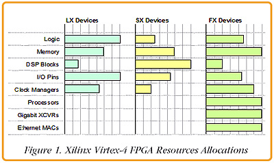
All the resources described so far are available in all Virtex-4 devices, but the ratio of these resources differs significantly among the three groups. Figure 1 shows the relative strengths of resources for each of the three classes of devices for the larger devices in each class. The LX devices deliver the most logic and I/O; the SX devices aim at DSP with 512 XtremeDSP slices; and the FX class offers generous memory and three other important resources found only in that family.
The first is on-board IBM 405 PowerPC processor cores that can be used as local microcontrollers to implement complete systems on a chip. They often eliminate the need for an external CPU for high-level supervisory functions.
The second resource is a set of serial gigabit transceivers backed up with serializer/deserializer logic and capable of handling bit rates up to 10 GHz. By configuring these interfaces through available IP cores, the FPGA supports popular high-speed serial standards and switched serial fabrics including Serial RapidIO, PCI Express, FibreChannel, SATA, SONET, and many others.
The third resource, unique to the FX group, is a set of 802.3 compliant Ethernet media access controllers (MACs). These support 10/100/1000 Base-x transmit/receive interfaces to system peripherals and are especially useful to the embedded PowerPC processors as a standard communication link to the outside world.
Embedded System Board Design
Virtually all board level products for open-architecture embedded systems introduced in the last few years, have taken advantage of FPGAs for the many features and benefits outlined above. FPGAs not only handle multiple types of interfaces to components, buses and communication links; they can also perform real-time DSP tasks required in demanding applications such as data acquisition, software radio, secure communications, and radar systems.
When embarking upon a new product design, the two main questions product managers and design engineers must answer when selecting the most appropriate FPGA are:
- Which FPGA best implements the board hardware design requirements, and
- Which FPGA best suits the extra features expected to be added by the customer
The first question has many facets but is often easier to answer. Usually, all components and interfaces on the board are either handled by or connected to the FPGA. This includes memory, clock and timing signals, ASICs, A/D and D/A converters, digital interfaces, buses, and communication links. The FPGA also incorporates several control and status features like registers, data multiplexers, counters, and state machines to instrument the control software libraries and drivers supplied with the product.
In some applications, the customer can use the product as is, without adding any custom IP to the FPGA. This, of course, makes the second question entirely moot. However, in this case, the unused resources in the FPGA become extra baggage and add to the product cost. Fortunately, different-density FPGA devices within a family often share a common package or printed circuit board pattern. This allows a single board design to use a simpler and less expensive FPGA when the customer needs no additional IP. The design still accommodates a larger device when extra FPGA resources are needed.
When the customer does want to add IP, the second question above can be even more difficult to answer than the first. This is because each customer invariably wants to implement something unique to his or her application.
Software Radio Board Example
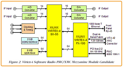
As mentioned previously, software radio products are a natural fit for FPGA technology. The PMC/XMC module shown in Figure 2, illustrates a product encompassing many essential features of software radio.
Two A/D converters and two D/A converters provide analog IF (intermediate frequency) signal interfaces to external analog RF up and downconverters and RF amplifiers for ultimate connection to the antenna. Real-time digital signal processing tasks such as digital up and downconversion, modulation and demodulation, encoding and decoding, and other operations are often all performed by the FPGA.
Large memory offered by the DDR2 SDRAM supports a circular buffer for implementing a digital delay memory, very useful in signal intelligence applications. In this mode, the accesses are sequential so efficient block transfers can deliver real-time storage and readback at the full sample rate for both channels. The QDR memory is a smaller SRAM with fast access to non-sequential memory locations. This type of memory is ideal for two-dimensional array processing where rows and columns of matrices need to be accessed equally fast. As a PMC module, a PCI bus interface must be included along with DMA controllers and FIFO buffers.
As an XMC module, the unit must include gigabit serial transceivers and some facility for implementing a serial fabric and/or protocol. Lastly, a front panel Ethernet port is extremely useful for control, status and communication functions to virtually any external computer system.
Selecting the Right FPGA
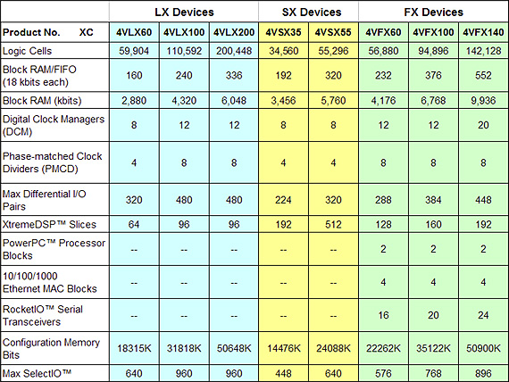
The FX family of Virtex-4 devices has all the necessary features required for these board attributes. Therefore, it becomes an obvious choice for this product. Nevertheless, the FX family is quite limited in DSP capability compared to the SX family. The table on the right shows exact quantities of resources for eight representatives from the 17 parts in the three device groups.
Even the largest member of the FX family has the same number of XtremeDSP slices as one of the smaller SX devices. Since customer access to ample DSP horsepower is a critical factor, an SX55 device is added to the PMC module, significantly boosting the total quantity of DSP slices by 512 from 192 to 704.
Since the SX55 must perform digital signal processing on real-time signals to and from the A/D, D/A, QDRAM and SDRAM, these components are attached directly to it. The FX100 is the natural choice for the PCI interface, the gigabit serial interface and the Ethernet port.
The PCI interface uses an off-the-shelf IP core installed in the FX100. It offers a fully compliant PCI 2.2 PCI bus interface using appropriate Virtex I/O pin interfaces. The local side of the PCI core is augmented with a custom 9-channel DMA engine and FIFO buffers, all tailored to the specific needs of the resources on the module.
The XMC interface utilizes the gigabit transceivers (called RocketIO) by grouping four serial bit lanes to form a "4x" port. Operating at a bit rate of 3.125 GHz, the resulting transfer rate is 1.25 Gbytes/sec in and out for each port. A second 4x port doubles this rate for the module, providing an extremely fast path to the carrier board.
Two 64-bit data buses joining the two FPGAs utilize the source-synchronous digital interfaces for moving data between them at extremely high rates. This supports direct streaming transfers for the XMC ports, which thus become capable of delivering full-rate data to and from A/D and D/A at the maximum sampling rate.
The resulting module design offers a highly configurable software radio building block because of the wealth of FPGA resources. Since the FPGA devices share common footprints with other family members, it is possible to substitute parts to tailor the board for a range of processing, cost, and power requirements.