Choosing the Right Mezzanine Module for Embedded Systemsby Rodger Hosking, Pentek, Inc.
Open architecture embedded systems for military/aerospace applications have always relied on mezzanine or daughter cards to provide flexibility and modularity because they are very effective in handling the large breadth of I/O functions required. Thanks to widespread adoption of industry standards defining these mezzanine products, carrier boards are able to accept mezzanine boards from a wide range of vendors, each specializing in niche technologies and interfaces.
Today, three popular mezzanine standards dominate the embedded market:
- PMC (PCI Mezzanine Card)
- XMC (Switched Mezzanine Card)
- FMC (FPGA Mezzanine Card)
These mezzanines support all popular industry architectures including VME, VXS, VPX, AMC, CompactPCI®, and CompactPCI Serial for both 3U and 6U form factors, and across a range of cooling techniques and ruggedization levels – especially important for MIL/AERO electronics. Each of these three mezzanine standards presents a unique set of advantages and disadvantages, which are discussed in this article.
Mezzanine Module Standards
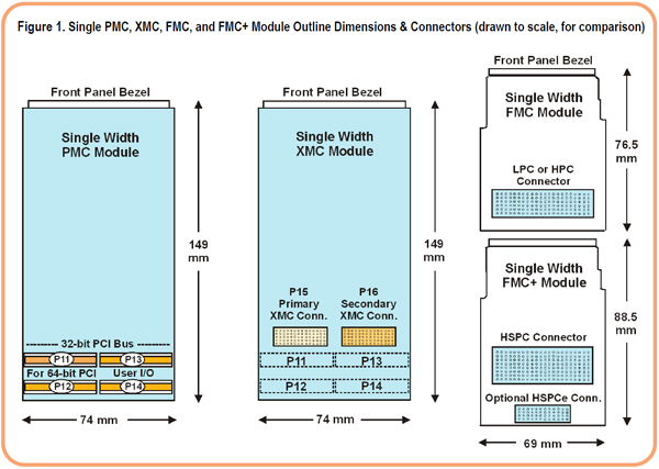
Defined under the IEEE 1386.1 standard more than 15 years ago, PMC uses the mechanical dimensions of the CMC (Common Mezzanine Card) from IEEE 1386 with the addition of up to four 64-pin connectors to implement a 32- or 64-bit PCI bus as well as user I/O.
Two connectors, P11 and P12 (see Figure 1), handle a 32-bit PCI bus, expandable to 64 bits with the addition of the P13 connector. Operating at PCI bus clock speeds of 33 or 66 MHz, the 32-bit interface delivers a peak transfer rate of 132 or 264 MB/sec, respectively, and twice that for a 64-bit interface.
A later extension, called PCI-X, boosts the clock rate to 100 or 133 MHz for a peak transfer rate of 800 or 1000 MB/sec for 64-bit implementations. The optional P14 connector supports 64 bits of user-defined I/O. As interconnect technology for massmarket PCs began shifting away from parallel PCI buses towards the faster PCIe (PCI Express) gigabit serial links, the need for a similar migration for mezzanine modules became apparent.
XMC modules are defined under VITA 42 as the switched fabric extension of the PMC module. It requires either one or two multi-pin connectors called the primary (P15) and secondary (P16) XMC connectors shown in Figure 1. Each connector can handle eight bidirectional serial lanes, using a differential pair of pins for each direction. The VITA 42.3 sub-specification defines pin assignments for PCIe, while VITA 42.2 covers SRIO (SerialRapidIO).
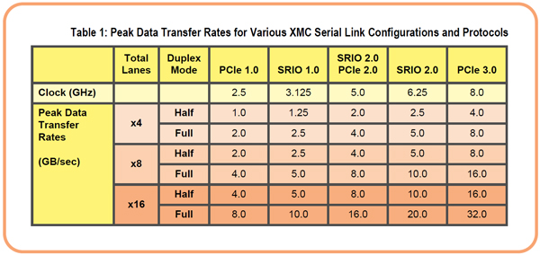
Typically, each XMC connector is used as a single x8 logical link or as two x4 links, although other configurations are also defined. Data transfer rates for XMC modules depend on the gigabit serial protocol and number of lanes per logical link. Table 1 shows the peak rates for different configurations and protocols, which compare favorably with peak PMC rates.
FMC modules are defined in the VITA 57 specification and are intended as I/O modules for FPGAs. They depart from the CMC form factor, with less than half the real estate, as shown in the top right of Figure 1. Two different connectors are supported: a low pin-count (LPC) connector with 160 contacts and a high pin-count (HPC) connector with 400 contacts. Connector pins are generically defined for power, data, control and status with specific implementation depending on the design.
FMC modules rely on the carrier board FPGA to provide the necessary interfaces to the FMC components. These can be single-ended or differential parallel data buses, gigabit serial links, clocks and control signals for initialization, timing, triggering, gating, and synchronization. For data, the high-density FMC connector provides 80 differential pairs or 160 singleended lines. It also has 10 high-speed gigabit serial lanes, with differential pairs for each direction.
In order to support the new class of data converter devices that use JESD204B gigabit serial interfaces instead of parallel LVDS, the FMC specification has been enhanced to FMC+. Defined in VITA 57.4, it increases the number of gigabit serial lanes from 10 to 24 through a new, higherspeed version of the HPC connector with four more rows of pins. The new connector for FMC+ is rated for data rates up to 28 Gbits/sec.
VITA 57.4 optionally adds 8 more gigabit serial lanes to the FMC+ module by extending the length of the original FMC module by 12 mm to support a new 40-pin connector, as shown in the bottom right of Figure 1. This boosts the total number of full-duplex gigabit serial lanes to 32 when maximum I/O data rates are required.
It should be noted that all three of these mezzanines are also available in doublewidth versions, fully defined in the specifications. This provides additional real estate for more components. However, the vast majority of mezzanines available in the marketplace today are single-width designs.
Lastly, all three specifications (PMC, FMC, and FMC) include complete specifications for rugged and conduction-cooled versions of these mezzanine products so they can be deployed in extreme MIL/AERO environments.
Data Transfer Capabilities
Regarding the data transfer rates, PMC and XMC modules are well determined by the interface standard installed. Nevertheless, these rates are often affected by the carrier board in several ways. A shared PCI bus supporting other traffic will effectively block all transfers to a PMC until it is granted use of the bus. For example, this problem occurs on dual PMC SBCs (single board computers) where the two PMCs often share the same local PCI bus.
Also, when PMCs are installed on simple 3U CompactPCI carriers, the common PCI backplane must be shared across all boards installed in the card cage. Lastly, a carrier card or adapter that presents a lower speed PCI bus to the PMC module will force the module to operate its interface at that lower speed.
XMCs have an inherent data rate advantage over PMCs because they use fast gigabit serial links. Even the slowest x4 PCIe 1.0 interface still matches the fastest PCI-X 64-bit bus at 133 MHz. However, a major system level implication for the gigabit serial interfaces is that they are dedicated point-to-point links and are not subject to the sharing penalty of parallel buses. Table 1 (above) shows the peak data transfer rates for PCIe and SRIO for different width gigabit serial links.
Ultimately, any system will have CPU and memory bandwidth limitations, but new multi-core processors and chip sets feature more than 40 PCIe Gen3 lanes, each handling 1 GB/sec, and four DDR3 memory banks, each delivering transfer rates of 12.8 GB/sec. In these systems, a dedicated x8 PCIe link between the XMC and the system supports a respectable transfer rate of 8 GB/sec.
Unlike PMCs and XMCs, FMCs do not use industry standard interfaces like PCI or PCIe. Instead, each FMC has a unique set of control lines and data paths, each one differing in signal levels, quantity, bit widths, and speed. At a 1 GHz data clock rate, the 80 differential data lines can deliver 10 GB/sec, although the new FMC+ specification doubles these rates.
The original FMC specification set a design goal of 10 Gbits/sec for each of the ten serial lanes, delivering peak aggregate data rates of 10 GB/sec. The new FMC+ specification of 28 Gbits/sec for a maximum of 32 serial lanes, boosts this aggregate peak data rate to nearly 90 GB/sec.
Real Estate and Power Considerations
FMC modules are less than half the size of PMCs and XMCs, and less real estate means less freedom to strategically place components for shielding, isolation and heat dissipation. For example, A/D converters are extremely sensitive to spurious signal pickup from power supplies, voltage planes, and adjacent copper traces. Often, the required power supply lines must be re-regulated and filtered locally on the same board as the A/D converters for best results, rather than on the carrier board. Arranging this circuitry on a small FMC module can be challenging. Even though XMC modules have more components, they can often be rearranged more easily because of the larger board size.
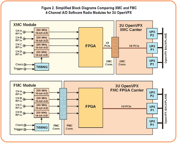
FMCs require the FPGA to reside on the carrier board, while FPGA-based XMC modules include the FPGA on the mezzanine board. Schematically, the overall circuitry between the front end and the system bus may be nearly identical, but the physical partitioning occurs at two different points.
To illustrate this, Figure 2 shows two different implementations of a 4-Channel A/D converter software radio module for 3U OpenVPX™, highly suitable for MIL/AERO applications. Notice that both block diagrams feature the same A/D converters and FPGAs and provide the same x8 PCIe interface to the OpenVPX backplane. The XMC implementation on top uses the XMC connector between the FPGA and the backplane, while the FMC implementation below uses the FMC connector between the A/Ds and the FPGA.
Because most of the power is consumed by the FPGA, comparing power dissipation between FMC and XMC modules will strongly favor the FMC. However, since the same resources are used in both block diagrams, the overall 3U module power dissipation is nearly identical.
In a comparison among PMC, XMC, and FMC modules, there is one additional factor. Gigabit serial interfaces implemented in FPGAs typically consume more power than parallel bus interfaces. So when considering PMC products versus XMC/FMC products, the PCI bus of the PMC module will typically draw less power than a PCIe link. Of course, the extra power required for PCIe delivers tremendous benefits in both speed and connectivity.
Software and FPGA Development Issues
Each FMC presents a unique electrical interface that must be connected to an FPGA configured precisely to handle that specific device. This may be a reasonable solution if the FMC module and the FMC carrier are both supplied by the same vendor, and the FPGA on the carrier is preconfigured by the vendor for the specific FMC module installed.
For 6U carriers with two or three FMC sites, the FPGAs must be configured to match the specific combination of each of the FMC modules installed at each site. This FMC-to-FPGA dependency creates a potentially large number of combinations resulting in configuration management and customer support issues. It may mean longer delivery times for first-time combinations, and higher costs. Also, the vendor may not offer an FMC carrier for the desired form factor or system architecture required.
When a customer purchases an FMC module from one vendor and an FMC carrier from a different vendor, additional challenges arise. Someone must develop custom FPGA configuration code for the carrier to support the FMC module. Perhaps the FMC vendor will agree to develop code for a third-party carrier. Perhaps the carrier vendor will develop code for a third party FMC module.
Failing either of these strategies, the customer must configure the FPGA himself, or hire a consultant to do the job. In this case, both the FMC module and the FMC carrier are third-party products with two different technical support resources. If something doesn't work, it can be difficult to resolve problems in an efficient and effective way. And, if either the FMC module vendor or the FMC carrier vendor should revise his product, it may affect the interoperability of the two boards.
Perhaps the most challenging aspect of FMCs is the development of software drivers and board support libraries covering the myriad combinations of modules and carriers. Unless this is supplied from a single vendor who also supplies the FMC module and carrier, the same support and development issues discussed above for FPGA development may arise.
In contrast, PMCs and XMCs use industry standard system interfaces, typically PCI and PCIe, with a strong trending towards XMCs with PCIe. Nearly all recent embedded systems take advantage of the widely-adopted PCIe standard for interconnecting system elements. This includes VXS, VPX, AMC, and CompactPCI, as well as high-performance PC platforms using PCIe cards installed in motherboard expansion slots.
Since PCIe is the system interface on most XMCs, they can be installed directly or with simple mechanical adaptors into all of these system architectures. Most importantly, these adapters can be obtained from a variety of vendors since they are simply redirecting the PCIe bus, thus eliminating the need for anyone to develop custom FPGA code for new combinations.
Device drivers and application software developed for popular embedded operating systems simply work, regardless of the architecture. This is due to the inherent connectivity of PCIe through bridges, switches, extender cables and expansion chassis regardless of the form factor of the boards, modules and backplanes.
All of these factors greatly reduce dependency on the XMC vendor and problems resolving multi-vendor responsibility. XMCs take advantage of an industry standard system interface, eliminate the need for custom FPGA development, easily support a wide range of system architectures, and come with complete software drivers and board support libraries. This can result in dramatic savings in systems integration and software development costs so important to MIL/AERO program budgets and schedules.
3U VPX XMC-Based Example
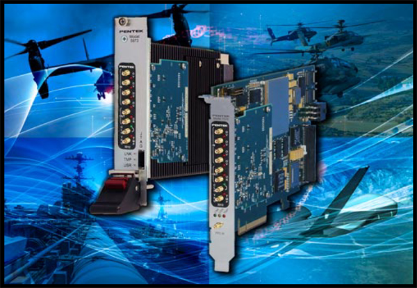
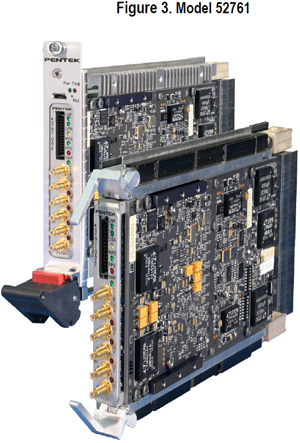
Figure 3 shows two Pentek Onyx® Model 52761 3U VPX modules that consist of an XMC module mounted on a simple VPX carrier, like the top diagram in Figure 2. The Model 71761 XMC module exploits the latest Virtex®-7 FPGA technology and features four 200 MHz 16-bit A/Ds and four multiband digital downconverters.
It is equipped with dual XMC connectors, each capable of supporting 8 lanes of gigabit serial links. The standard product uses one of these connectors for a PCIe Gen 3.0 x8 interface, delivering a peak data transfer rate of 8 GB/sec through the 3U VPX carrier to the VPX backplane.
Two versions of this product are shown: the top one is for air-cooled systems and the bottom one is for conduction-cooled systems.
As a testament to their versatility, Pentek XMC modules are also available in PCIe, CompactPCI, 6U VPX, and AMC form factors by using other adapters, and are supported with ReadyFlow® Board Support Libraries for Windows, Linux, and VxWorks.
|
|
Customers wishing to add custom IP for signal processing or special algorithms can choose the GateFlow® FPGA Design Kit containing full VHDL source code and the complete FPGA project. However, many customers take advantage of the rich collection of factory-installed FPGA functions addressing communications and radar applications, saving the need for custom FPGA development.
3U VPX FMC-based Module
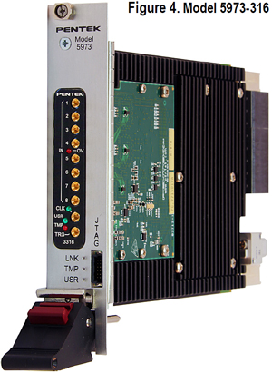
Figure 4 shows an air-cooled Model 5973-316 3U VPX FlexorSet® module consisting of a Model 3316 FMC mounted in a 3U VPX FMC carrier, like the bottom diagram in Figure 2.
The Model 3316 FMC has eight 250 MHz 16-bit A/Ds with full synchronization between channels and across other modules. This high channel-density solution is ideal for phased array radar and software radio applications.
The 3U VPX FMC carrier contains a Virtex-7 FPGA which accepts data from the FMC A/Ds, performs optional digital down conversion, and a PCIe Gen 3 x8 system interface to the VPX backplane.
In fact, the circuitry for the Model 52761 in Figure 3 and the Model 5973-316 in Figure 4 are quite similar, illustrating the equivalency of the XMC and FMC architectures when applied to VPX products.
|
|
Pentek's combination of FMC modules and FMC carriers are offered as FlexorSets. These complete sub-systems include factory-installed FPGA code to optimize the features. Like XMC modules, Pentek offers ReadyFlow Board Support Libraries for C-language development, and the GateFlow FPGA Design Kit for userdefined IP development.
The FlexorSet approach nicely solves traditional problems inherent in FMC technology: compatibility issues between FMC modules and carriers, developing custom FPGA configuration code, and the lack of tools for software development.
Summary
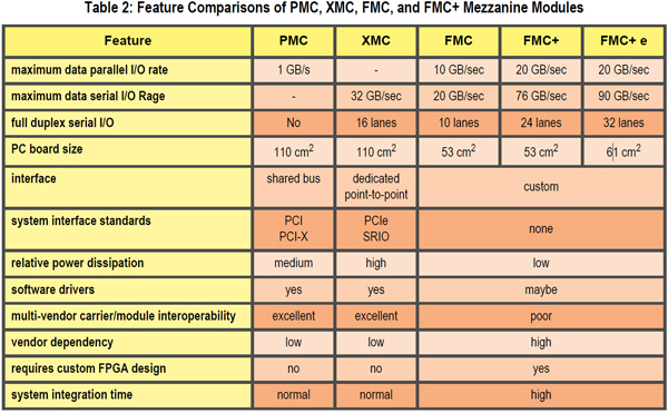
Table 2 summarizes the points discussed in this article, comparing PMC, XMC, FMC, and FMC+ modules. Military and aerospace system integrators must weigh the pros and cons of each, remembering that all three are available in rugged versions suitable for deployment in severe environments. With hundreds of vendors and thousands of products, designers have many available choices.
FMC modules can be quite effective as long as the same vendor supplies both the mezzanine module and the carrier with tested and installed FPGA configuration code, like FlexorSet offerings. Otherwise, XMC modules offer excellent solutions for embedded systems due to the proliferation of links, carriers, backplanes, and adaptors all based on PCIe. This eliminates the need for a custom FPGA development effort for each new application, minimizes product support issues, and speeds development cycles.
|